- 您现在的位置:买卖IC网 > Sheet目录17368 > NCP3011GEVB (ON Semiconductor)BOARD EVAL NCP3011 BUCK CTLR
�� �
�
�NCP3011,� NCV3011�
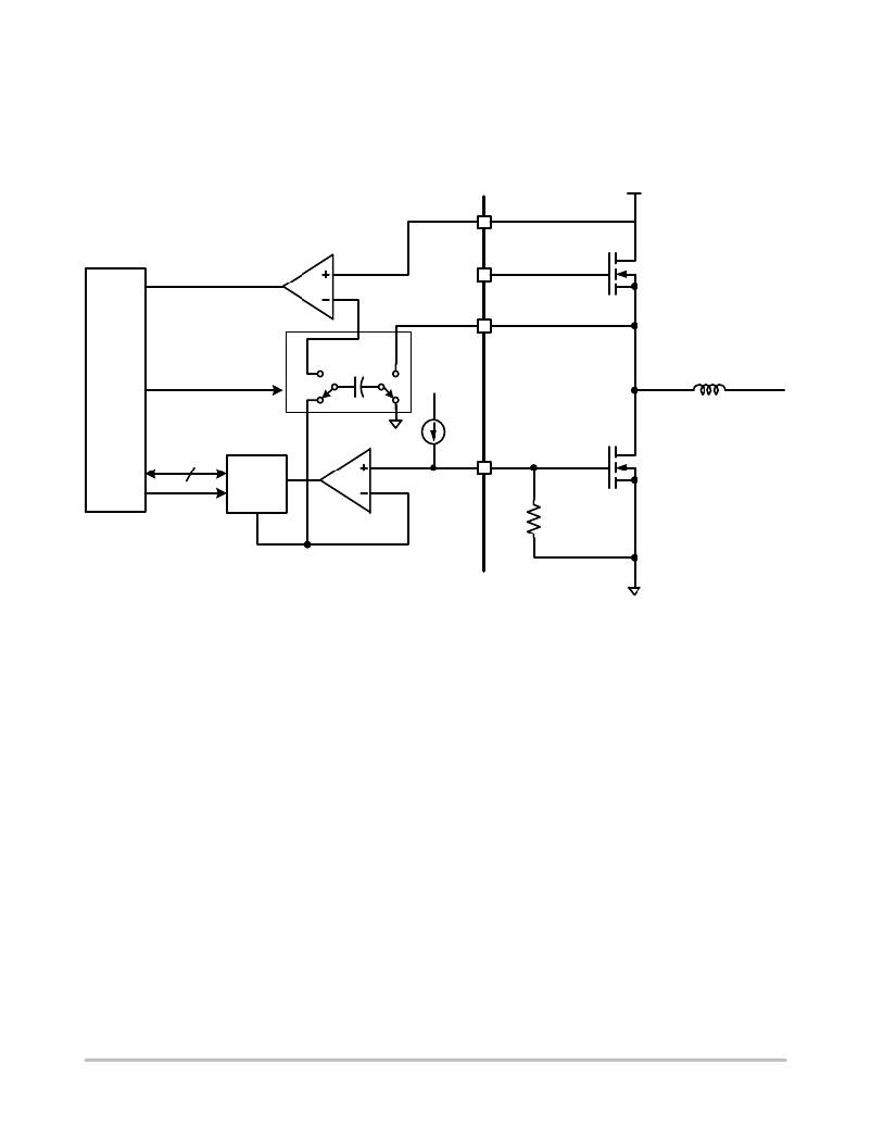
�CURRENT� LIMIT� AND� CURRENT� LIMIT� SET�
�Overview�
�The� NCP3011� uses� the� voltage� drop� across� the� High� Side�
�MOSFET� during� the� on� time� to� sense� inductor� current.� The�
�I� Limit� block� consists� of� a� voltage� comparator� circuit� which�
�compares� the� differential� voltage� across� the� V� CC� Pin� and� the�
�V� SW� Pin� with� a� resistor� settable� voltage� reference.� The� sense�
�portion� of� the� circuit� is� only� active� while� the� HS� MOSFET�
�is� turned� ON.�
�VI� N�
�VCC�
�CONTROL�
�6�
�Ilim� Out�
�DAC� /�
�COUNTER�
�VSense�
�Itrip� Ref�
�Switch�
�Cap�
�Iset�
�13� uA�
�Vset�
�HSDR�
�VSW�
�LSDR�
�RSet�
�Itrip� Ref� ?� 63� Steps,� 6.51� mV/step�
�Figure� 36.� I� set� /� I� Limit� Block� Diagram�
�Current� Limit� Set�
�The� I� Limit� comparator� reference� is� set� during� the� startup�
�sequence� by� forcing� a� typically� 13� m� A� current� through� the�
�low� side� gate� drive� resistor.� The� gate� drive� output� will� rise�
�to� a� voltage� level� shown� in� the� equation� below:�
�V� set� +� I� set� *� R� set� (eq.� 4)�
�Where� I� SET� is� 13� m� A� and� R� SET� is� the� gate� to� source� resistor�
�on� the� low� side� MOSFET.�
�This� resistor� is� normally� installed� to� prevent� MOSFET�
�leakage� from� causing� unwanted� turn� on� of� the� low� side�
�MOSFET.� In� this� case,� the� resistor� is� also� used� to� set� the�
�I� Limit� trip� level� reference� through� the� I� Limit� DAC.� The� I� set�
�process� takes� approximately� 350� m� s� to� complete� prior� to�
�Soft� ?� Start� stepping.� The� scaled� voltage� level� across� the� I� SET�
�resistor� is� converted� to� a� 6� bit� digital� value� and� stored� as� the�
�trip� value.� The� binary� I� Limit� value� is� scaled� and� converted� to�
�the� analog� I� Limit� reference� voltage� through� a� DAC� counter.�
�The� DAC� has� 63� steps� in� 6.51� mV� increments� equating� to� a�
�maximum� sense� voltage� of� 403� mV.� During� the� I� set� period�
�prior� to� Soft� ?� Start,� the� DAC� counter� increments� the�
�reference� on� the� I� SET� comparator� until� it� crosses� the� V� SET�
�voltage� and� holds� the� DAC� reference� output� to� that� count�
�value.� This� voltage� is� translated� to� the� I� Limit� comparator�
�during� the� I� Sense� portion� of� the� switching� cycle� through� the�
�switch� cap� circuit.� See� Figure� 36.� Exceeding� the� maximum�
�sense� voltage� results� in� no� current� limit.� Steps� 0� to� 10� result�
�in� an� effective� current� limit� of� 0� mV.�
�Current� Sense� Cycle�
�Figure� 37� shows� how� the� current� is� sampled� as� it� relates�
�to� the� switching� cycle.� Current� level� 1� in� Figure� 37�
�represents� a� condition� that� will� not� cause� a� fault.� Current�
�level� 2� represents� a� condition� that� will� cause� a� fault.� The�
�sense� circuit� is� allowed� to� operate� below� the� 3/4� point� of� a�
�given� switching� cycle.� A� given� switching� cycle’s� 3/4� T� on�
�time� is� defined� by� the� prior� cycle’s� T� on� and� is� quantized� in�
�10� ns� steps.� A� fault� occurs� if� the� sensed� MOSFET� voltage�
�exceeds� the� DAC� reference� within� the� 3/4� time� window� of�
�the� switching� cycle.�
�http://onsemi.com�
�17�
�发布紧急采购,3分钟左右您将得到回复。
相关PDF资料
MIC2505BM
IC SW HIGH SIDE SGL 2A 8SOIC
MIC2505-2BM
IC SW HIGH SIDE SGL 2A 8SOIC
MIC2505-1BM
IC SW HIGH SIDE SGL 2A 8SOIC
TAAB106K020G
CAP TANT 10UF 20V 10% AXIAL
MC34063LBBEVB
EVAL BOARD FOR MC34063LBB
A9BAG-0502F
FLEX CABLE - AFF05G/AF05/AFE05T
EBM08DTMD-S189
CONN EDGECARD 16POS R/A .156 SLD
RCM06DSUI
CONN EDGECARD 12POS DIP .156 SLD
相关代理商/技术参数
NCP3012
制造商:ONSEMI 制造商全称:ON Semiconductor 功能描述:Synchronous PWM Controller
NCP3012DTBR2G
功能描述:电压模式 PWM 控制器 Single Output Buck 0.8V to 40V 70uA RoHS:否 制造商:Texas Instruments 输出端数量:1 拓扑结构:Buck 输出电压:34 V 输出电流: 开关频率: 工作电源电压:4.5 V to 5.5 V 电源电流:600 uA 最大工作温度:+ 125 C 最小工作温度:- 40 C 封装 / 箱体:WSON-8 封装:Reel
NCP301HSN09T1
功能描述:电压监测器/监控器 0.9V Detector RoHS:否 制造商:Texas Instruments 监测电压数:2 监测电压:Adjustable 输出类型:Open Drain 欠电压阈值: 过电压阈值: 准确性:1 % 工作电源电压:1.5 V to 6.5 V 工作电源电流:1.8 uA 最大工作温度:+ 125 C 封装 / 箱体:SON-6 安装风格:SMD/SMT
NCP301HSN09T1G
功能描述:电压监测器/监控器 0.9V Detector w/Reset High RoHS:否 制造商:Texas Instruments 监测电压数:2 监测电压:Adjustable 输出类型:Open Drain 欠电压阈值: 过电压阈值: 准确性:1 % 工作电源电压:1.5 V to 6.5 V 工作电源电流:1.8 uA 最大工作温度:+ 125 C 封装 / 箱体:SON-6 安装风格:SMD/SMT
NCP301HSN10T1
制造商:ONSEMI 制造商全称:ON Semiconductor 功能描述:Voltage Detector Series
NCP301HSN11T1
制造商:ONSEMI 制造商全称:ON Semiconductor 功能描述:Voltage Detector Series
NCP301HSN12T1
制造商:ONSEMI 制造商全称:ON Semiconductor 功能描述:Voltage Detector Series
NCP301HSN13T1
制造商:ONSEMI 制造商全称:ON Semiconductor 功能描述:Voltage Detector Series